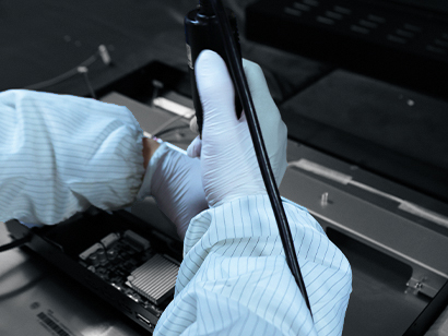
The manufacturing process of an LCM display module encompasses a complete system from glass substrate to final product. Each step undergoes stringent parameter control, directly determining the panel's image uniformity, signal stability, and long-term reliability under harsh environments.
In the LCD industry, the precision of its manufacturing chain has become a core competitive advantage. This article will systematically break down the LCD-related components of an LCM module.
Understanding the details of these processes will help industry professionals more accurately grasp the technical essence of LCD displays and make rational judgments during the selection process.
What Is LCD?
An LCD stands for Liquid Crystal Display. Its core working principle is based on the selective selection of liquid crystal molecules under the influence of an electric field, which precisely controls the transmittance of backlight to form an image.
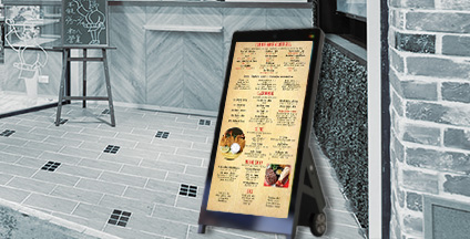
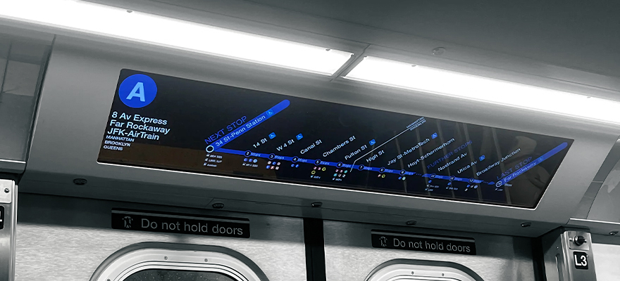
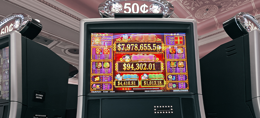
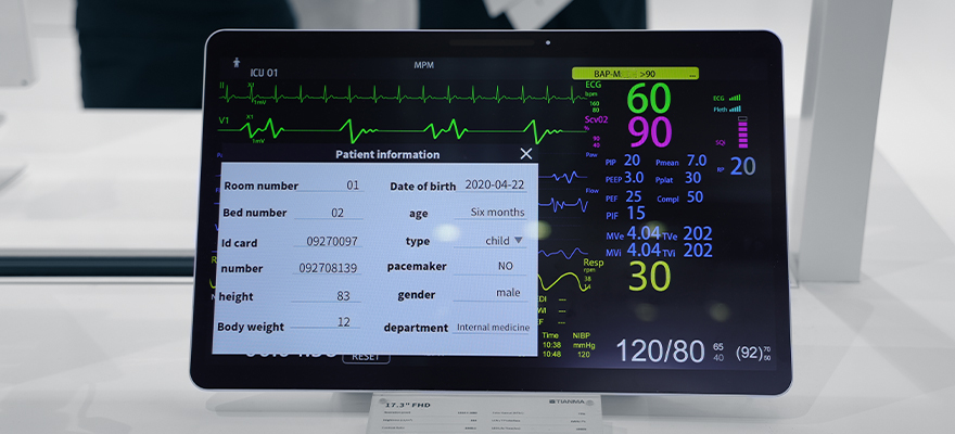
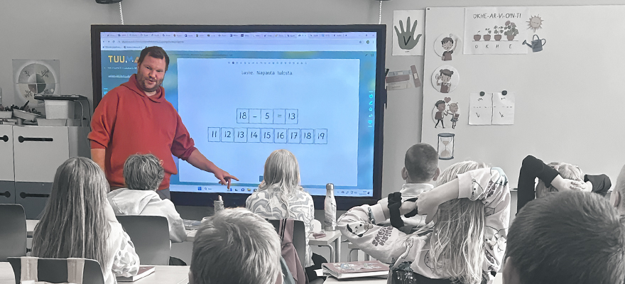
It is currently the most mature and cost-effective technology in the commercial display field, widely used in industrial control equipment, medical instruments, advertising displays, and conference tablets. Next, we will describe the manufacturing process of LCDs.
Pre-processing Cleaning Process
This is a core process before LCD processing. Thoroughly cleaning the glass before the critical LCD manufacturing steps removes particles, oil, and impurities, ensuring film adhesion and process uniformity. This improves the yield rate of the finished product and, to a certain extent, avoids display defects.
Photoresist Coating Process
A layer of photoresist is uniformly coated onto the ITO glass surface. The thickness, flatness, and particle size must be controlled within the micrometer level.
This photoresist layer will later become the mask layer for subsequent exposure, development, and etching, laying the foundation for micrometer-level pattern transfer. This is a key process that determines the precision and yield of the panel's circuitry.
Developing/Hardening Process
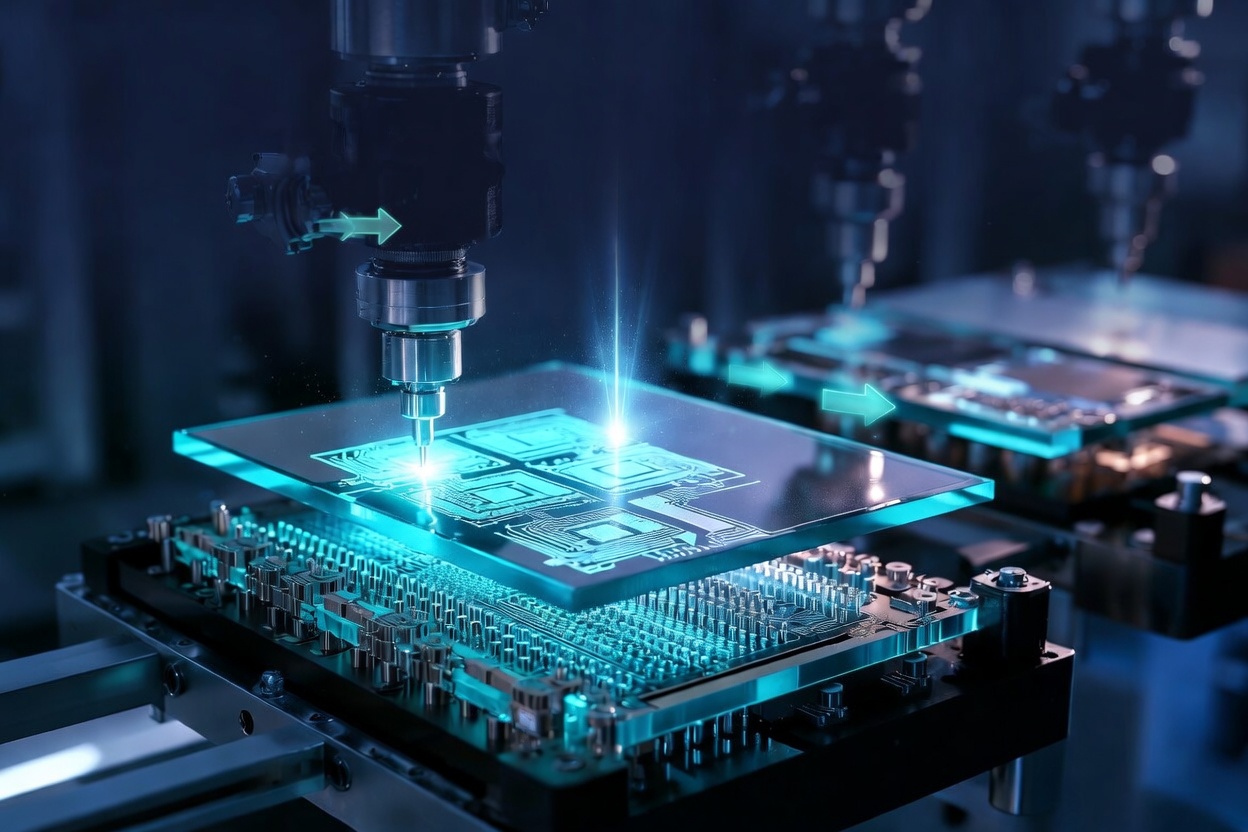
Exposure involves using ultraviolet light to pass through a precision photomask and accurately transfer the designed circuit pattern onto the photoresist. This step is a core and critical process that determines the accuracy of the circuitry and the yield rate of the panel.
Exposure Process
Developing reveals the exposed pattern, forming a complete circuit mask; while hardening involves high-temperature baking to improve the hardness and adhesion of the photoresist, enhancing its adhesion and etching resistance. Both processes ensure that subsequent etching produces precise and complete circuits.
Acid Etching Process
The acid etching process uses a precisely proportioned acidic solution to precisely etch away excess metal, forming the driving circuitry and traces of the LCD. This step directly determines the circuit accuracy, conductivity, and panel yield.
Cleaning Process Before Demolding/Pad Printing
After etching, the photoresist in the remaining LCM LCD module must be completely removed. This step is to prepare for subsequent PI coating.
TOP/PI Pad Printing Process
An alignment film and protective layer are coated on the surface of the array glass.
This acts as a "compass" for the alignment of liquid crystal molecules, ensuring uniform film thickness and consistent orientation.
This guarantees display quality, viewing angle, and no image retention, and is a key film formation process before the LCD is turned on.
Friction Process
The friction process refers to rubbing microgrooves in a uniform direction onto the PI film, allowing liquid crystal molecules to align neatly in a fixed direction.
This is a key process that determines the display effect, uniformity, and presence of image retention in LCDs.
Epoxy Frame Printing / Conductive Adhesive / Powder Coating
This process has three steps: Epoxy frame printing seals and bonds the two glass pieces together.
Conductive adhesive printing establishes electrical conductivity between the upper and lower substrates.
Powder coating supports cell thickness and ensures uniform display. All three processes prepare the cell for final assembly.
These three processes collectively determine whether the panel leaks, short-circuits, or has uniform cell thickness.
Lamination and Hot Pressing Process
This process requires precise alignment and bonding of the TFT and CF substrate in a vacuum environment to seal the liquid crystal.
Then, the epoxy frame is cured by hot pressing to ensure the panel is firm and leak-proof. These two processes are crucial to the success of cell assembly and directly determine the yield, cell thickness, and reliability.
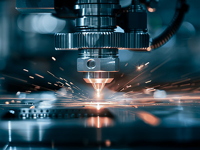
Cutting/Splitting Process
A high-precision cutting wheel is used to carve shallow grooves into a large-size LCD panel, and then the panel is precisely split along the grooves.
The cut surface must be flat, without chipped edges or hidden cracks, laying a good foundation for the entire machine.
Liquid Filling/Leveling Process
The liquid crystal is injected into an empty cell, and then leveled by heating and applying electricity to ensure even distribution of the liquid crystal and eliminate air bubbles.
This step directly determines whether the image has mura (highlighting effect).
LCD Cleaning And Aging Process
LCD cleaning first thoroughly removes residual adhesive, liquid, and dust to ensure appearance and bonding yield.
Then, it undergoes high-temperature and high-humidity electrical aging to screen for early defects and stabilize the liquid crystal state.
This step can intercept over 90% of potential defects and is the core of reliability control.
Semi-finished Product QC Process
This involves a comprehensive inspection of the LCD panels after they have been assembled, including lighting, appearance, dimensions, and electrical properties.
Defects are intercepted early to prevent them from flowing into later stages and causing waste. It is a crucial quality checkpoint bridging the upstream and downstream processes.
Secondary Cleaning Plasma Process
The secondary cleaning of the OC panel removes visible dirt and grime. Plasma cleaning provides deep cleaning and surface activation, improving adhesion and bonding yield. Both processes are crucial for enhancing the adhesion of the polarizer and FPC.
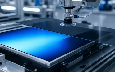
Surface Mount Technology
SMT involves attaching polarizing films to the top and bottom surfaces of an LCD panel. This is the core process that enables the panel to display images, directly determining the display effect, appearance, and module yield.